Vector comparison of Panel-Level Packaging and Wafer-Level Packaging showing chip density and efficiency differences
The semiconductor industry sees fierce competition. Its leading giants battle over panel-level packaging (PLP). This advanced packaging technology is rapidly becoming a key focus. It promises to revolutionize chip manufacturing. PLP offers significant advantages over traditional wafer-level packaging (WLP). Demand for powerful, efficient, and compact devices is surging. This includes AI, 5G, and high-performance computing. PLP is crucial for the next generation of semiconductors.
The Shift to Panel-Level Packaging: Why It Matters
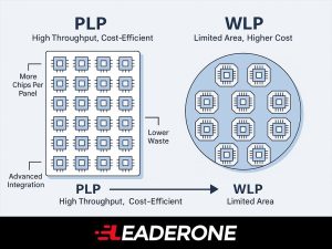
Panel-level packaging involves assembling multiple semiconductor dies. It also includes system-in-packages (SiPs). These are placed on large, rectangular panels. These panels are like those used in PCB manufacturing. This differs from circular wafers. This fundamental shift in form factor offers several compelling benefits:
- Enhanced Efficiency and Cost Reduction: PLP’s larger surface area allows more chips to be processed at once. This leads to higher throughput. It also reduces manufacturing costs per chip. This is vital for high-volume production.
- Optimal Material Utilization: Rectangular panels minimize material waste. Circular wafers often have underutilized corners.
- Improved Integration and Performance: PLP helps with advanced designs. These include System-in-Package (SiP) and heterogeneous integration. It allows seamless combination of various die technologies. Logic, memory, and RF can all be combined into one compact package. This is key for complex AI chipsets and other compute-intensive applications.
- Miniaturization and Form Factor Reduction: Densely packing components on panels helps create smaller, thinner devices. This supports the industry’s drive for miniaturization.
- Leveraging Existing Infrastructure: PLP manufacturing might use existing equipment. This includes tools for IC substrates, PCBs, and LCDs. This could lower investment and speed up development.
Key Players and Their Strategies
The battle for PLP leadership involves industry titans. These include TSMC, Samsung, and Intel. Each company has distinct strategies. They are investing heavily in research and development:
- TSMC: The Taiwanese foundry giant is actively developing its PLP technology. They are exploring glass as a panel material. TSMC aims to expand its advanced packaging capacity significantly, including CoWoS. They view PLP as a “radically new” technique. It will meet the escalating demands of AI chipsets. Their approach focuses on pushing integration and performance limits.
- Samsung: Samsung is a strong contender in both foundry and packaging. They have made big strides in PLP. Samsung acquired this business from Samsung Electro-Mechanics. Samsung reportedly focuses on plastic (organic) as the core panel material. They leverage their experience in packaging mobile APs and PMICs.
- Intel: Beyond chip manufacturing, Intel is a key player in advanced packaging. This includes glass core substrates (GCS). GCS is complementary to PLP due to similar panel sizes. Intel’s long-term R&D in GCS offers a new industry direction. It emphasizes enhanced performance and scalability for HPC and AI.
Other major players are also involved. These include OSATs (Outsourced Semiconductor Assembly and Test) like ASE, Amkor, and JCET. IC substrate and PCB manufacturers are investing too. They all aim to meet the growing demand for cost-effective advanced packaging solutions.
Overcoming the Hurdles
PLP offers compelling advantages. Yet, its widespread adoption faces challenges. These include technical and economic hurdles:
- High Costs and Complexity: Initial investment and PLP implementation can be substantial. It requires significant retooling. It also needs new processes and materials.
- Technical Challenges: Ensuring uniform processing across large panels is tough. Managing panel warpage is another issue. Achieving precise die placement accuracy is vital. Maintaining process uniformity impacts yield and cost-effectiveness.
- Yield Management: Chip shifting can greatly reduce yield rates. This requires strict control over the packaging process.
However, industry leaders are addressing these issues. Equipment manufacturers and material suppliers are also helping. The rapid evolution of AI and high-performance computing drives this. These fields demand larger, more complex packages. This strong impetus helps overcome obstacles. It pushes PLP towards mainstream adoption.