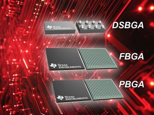
Real-world BGA package applications: DSBGA in mobile devices, NFBGA in industrial systems, PBGA in computing hardware
Demystifying BGA packaging: A comparative analysis of PBGA, NFBGA, and DSBGA focusing on size, pin density, and real-world applications.
In the intricate world of electronics design, selecting the appropriate integrated circuit (IC) package is a critical step that directly influences the final product’s form factor, performance, and reliability. Ball Grid Array (BGA) technology has emerged as a dominant packaging solution, particularly for high pin-count devices and applications demanding efficient thermal management. Within the BGA landscape, Plastic Ball Grid Array (PBGA), New Fine-Pitch Ball Grid Array (NFBGA), and Die-Size Ball Grid Array (DSBGA) represent three key variations. While all rely on an array of solder balls for electrical connection to the printed circuit board (PCB), their distinct characteristics make them suitable for different design scenarios.
Understanding the Basics: PBGA, NFBGA, and DSBGA
PBGA, NFBGA, and DSBGA are all categorized as surface-mount technology (SMT) packages. This means they are designed to be soldered directly onto the surface of a PCB, enabling the creation of smaller and more densely populated electronic assemblies. However, their internal structure and key specifications exhibit significant differences.
Key Differences Summarized:
Physical Footprint:
PBGA typically presents the largest physical footprint among the three. Its package body is designed to accommodate ICs with a moderate to high number of pins.
NFBGA offers a more compact footprint compared to PBGA. The reduced spacing between its solder balls allows for a greater number of pins within a smaller area.
DSBGA boasts the most minimal footprint, with its package dimensions being almost identical to the silicon die itself. This makes it the go-to choice for applications where space is at an absolute premium.
Solder Ball Spacing (Pitch):
PBGA features a relatively wider solder ball pitch, commonly ranging from 1.0 mm to 1.5 mm. This larger spacing can simplify the routing of electrical connections on the PCB.
NFBGA utilizes a finer solder ball pitch, typically less than 1.0 mm, such as 0.8 mm or 0.5 mm. This tighter spacing is a primary factor in its smaller size and higher pin density.
DSBGA employs the finest solder ball pitch, often ranging from 0.3 mm to 0.5 mm. This ultra-fine pitch is essential for direct interconnection with the die’s input/output pads within an extremely compact area.
Typical Use Cases:
PBGA is frequently chosen for applications where a balance of cost-effectiveness and performance is desired, such as in the main processors and chipsets found in desktop and some laptop computers.
NFBGA is commonly found in portable electronic devices like smartphones, tablets, and handheld gaming consoles where a small physical size and a significant number of input/output connections are crucial design considerations.
DSBGA is the preferred packaging solution for ultra-portable and highly space-constrained products like mobile phones, wearable devices, and memory cards where minimizing both size and weight is paramount.
Why These Differences Matter in Practice:
Maximizing Board Real Estate:
The incredibly small size of DSBGA enables the highest density of components on a PCB, a critical advantage in today’s miniaturized electronic products. NFBGA offers a significant space-saving benefit for portable designs, while PBGA is well-suited for applications with less stringent size limitations.
Optimizing Electrical Performance:
The direct die-to-PCB connection in DSBGA packages results in the shortest possible electrical pathways, leading to superior electrical performance and signal integrity, especially in high-frequency applications. NFBGA offers improved electrical characteristics compared to PBGA due to its smaller size and finer pitch.
Navigating Manufacturing Challenges:
The extremely fine pitch of DSBGA can introduce complexities in the manufacturing process, particularly during soldering and assembly. NFBGA also demands more precise manufacturing techniques than PBGA due to its smaller features. PBGA, with its larger and more spaced-out solder balls, generally offers more forgiving manufacturing tolerances.
In Simple Terms for Designers:
Think of PBGA as a robust and cost-effective general-purpose option. NFBGA is your go-to for making portable devices more compact while maintaining high pin counts. DSBGA is the ultimate solution when you absolutely need the smallest possible package footprint. Your choice will depend on the specific constraints and priorities of your electronic design project.