The relentless pursuit of smaller, faster, and more powerful microchips continues to drive innovation in the semiconductor industry. As humanity ventures further into the age of artificial intelligence, high-performance computing, and advanced connectivity, the demand for cutting-edge processing power intensifies. At the forefront of this technological race is the 1.4nm chip, representing the next frontier in silicon engineering. This incredibly tiny fabrication process promises to redefine what’s possible in electronics, but its development comes with immense technical and economic challenges.
What Does “1.4nm” Really Mean?
In the world of semiconductors, “nanometer” (nm) refers to the feature size of transistors on a chip. While once a direct measure of gate length, today it’s more of a marketing term or a generational indicator for a specific process node. A smaller nanometer number generally signifies higher transistor density, improved performance, and greater power efficiency. The leap to 1.4nm means packing an unprecedented number of transistors onto a single piece of silicon, unlocking new levels of computational capability.
The Race to 1.4nm: Who’s Leading the Charge?
The development of such advanced process nodes is a fiercely competitive arena dominated by a few global giants:
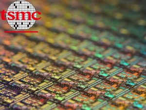
- TSMC (Taiwan Semiconductor Manufacturing Company): As the world’s largest contract chipmaker, TSMC is a major player in the 1.4nm race. They have reportedly unveiled their 1.4nm process technology, which they are calling “A14” (Angstrom 14), with plans for mass production by 2028. TSMC’s A14 node promises significant improvements over their 2nm chips, including higher speed at the same power and increased logic density. They are heavily investing in High-NA EUV lithography, a critical technology for achieving these ultra-fine resolutions.
- Samsung Electronics: Samsung Foundry, another key player, has also publicly stated ambitions for 1.4nm process technology. While recent rumors suggested they might re-evaluate their 1.4nm plans to focus on optimizing current 2nm/3nm nodes, their initial target for 1.4nm mass production was around 2027. Samsung is also utilizing Gate-All-Around (GAA) transistor architecture, which is crucial for scaling beyond current FinFET designs.
- Intel: Intel, a long-standing semiconductor innovator, is actively pushing its own advanced nodes. While their naming convention differs (e.g., 20A and 18A), they are striving to match or even surpass competitors in transistor density and performance. Intel aims for its “A14” (1.4nm equivalent) node around 2028.

The Immense Challenges of Manufacturing 1.4nm Chips
Creating chips at the 1.4nm scale is an engineering marvel, fraught with daunting challenges:
- Extreme Ultraviolet (EUV) Lithography: Manufacturing at such minuscule dimensions relies heavily on EUV lithography. For 1.4nm, even more advanced “High-NA EUV” machines are required. These machines are incredibly complex, costing hundreds of millions of dollars each, and are produced by only one company globally: ASML.
- Transistor Architecture: Traditional FinFET (Fin Field-Effect Transistor) designs reach their physical limits at these nodes. Companies are transitioning to Gate-All-Around (GAA) transistors, and potentially even more novel structures like complementary FETs (CFETs), to gain better control over current flow and reduce leakage.
- Yield Rates: Achieving acceptable yield rates (the percentage of functional chips from a wafer) becomes exponentially harder with smaller nodes. Even tiny defects can render a chip unusable.
- Cost and Investment: The research, development, and manufacturing infrastructure for 1.4nm chips demand colossal investments. Building and equipping a single advanced fabrication plant (fab) can cost tens of billions of dollars.
- Thermal Management: As more transistors are crammed into a smaller space, heat dissipation becomes a major hurdle. Innovative cooling solutions and advanced packaging techniques are crucial.
The Impact of 1.4nm Chips: A Glimpse into the Future
The successful development and mass production of 1.4nm chips will have a transformative impact across industries:
- Artificial Intelligence: More powerful and efficient AI accelerators will enable increasingly complex AI models to run faster, even on edge devices.
- High-Performance Computing: Supercomputers will achieve unprecedented computational speeds, accelerating scientific research and complex simulations.
- Consumer Electronics: Smartphones, laptops, and other portable devices will become even thinner, lighter, and more powerful, with extended battery life.
- Data Centers: Enhanced efficiency will lead to greener, more cost-effective data centers, supporting the growing cloud infrastructure.
- Automotive: Advanced autonomous driving systems will benefit from the real-time processing capabilities offered by these chips.
The 1.4nm chip is not just about a smaller number; it represents a monumental leap in human ingenuity and engineering. While challenges abound, the relentless pursuit of this technology promises a future where our electronic devices are more intelligent, responsive, and seamlessly integrated into our lives than ever before.